Inhero MR2 — Datasheet
Inhero MR2 – Smart Solar Mesh Board Hardware Revision 1.1
Board Overview
The Inhero MR2 is a LoRa mesh repeater board based on the RAK4630(H) module (nRF52840 + SX1262, high-band variant — see LoRa Frequency Bands) with integrated smart solar charging, power monitoring, and low-voltage protection. Supported battery configurations are 1S Li-ion, 1S LiFePO4, 2S LTO, and 1S Na-ion. The board was specifically designed for autonomous long-term deployment at remote or hard-to-reach locations. In Central Europe, uninterrupted continuous repeater operation is possible with unshaded solar panels ≥ 1 W and battery capacities ≥ 9 Ah.
The charge and discharge cutoff voltages (see table Supported Battery Chemistries) are chosen to avoid excessive stress on the batteries during summer while ensuring that sleep mode can be reliably initiated when energy is low.
In low-voltage sleep, current consumption is < 500 µA. Once the battery voltage has risen above the respective low-V wake threshold (see table Supported Battery Chemistries) through solar charging, the board boots normally. The 200 mV hysteresis between sleep and wake thresholds prevents motorboating – an uncontrolled, rapid on/off cycling of the system that would occur if the sleep and wake thresholds were too close together.
Safety & Protection Features
| Feature | Description |
|---|---|
| Watchdog Timer (WDT) | nRF52840 hardware watchdog. Automatically reboots the board if the firmware hangs – essential for unattended long-term operation. |
| Low-Voltage Protection | INA228 ALERT interrupt on chemistry-specific threshold → controlled System Sleep with RTC wake. Solar charging remains active during sleep (CE pin latched). |
| Charger requires active firmware | The BQ25798 only charges when the firmware is actively running. Without flashed firmware or with the 3.3V off switch engaged, charging remains disabled. The nRF52840 must be able to monitor the charger at all times as host. |
| JEITA Temperature Protection | Temperature-dependent charge current reduction via the NTC sensor (TS pin). Frost charge protection configurable via set board.fmax. LTO and Na-ion run with the temperature guard off (no JEITA supervision); for Na-ion the permissible charge temperature is set by the cell datasheet, not by the board. The Inhero voltage divider (RT1=5.6 kΩ, RT2=27 kΩ) shifts TS thresholds lower than TI reference (~2–3 °C; effective T-Cool range approx. −2 °C to +3 °C, see JEITA table in README). WARM zone configured to start at ~52 °C (register: 55 °C), effectively neutralized (VREG + ICHG unchanged in WARM), auto battery discharge disabled — see README.md — JEITA for details. Note: JEITA thresholds are evaluated by the BQ25798 directly in hardware. The set board.tccal calibration corrects only the CLI/telemetry temperature readout and does not affect JEITA behavior — see FAQ #12. |
| JEITA Override | set board.jeitaignore 1 sets the BQ25798 TS_IGNORE bit, so charging continues below the T-Cold threshold (≈ −2 °C). Off by default. Accepted for Li-ion 1S and LiFePO4 1S; effective only while board.batcap has been set and board.imax is at or below 0.05C of that capacity. With TS_IGNORE set the charge suspend at T-Hot (≈ +57.7 °C) is dropped as well. Frost charging Li-ion or LiFePO4 is at the operator's own risk and is scoped to Central European frost; sites regularly below −20 °C call for LTO or a Na-ion cell rated for charging there. See BATTERY_GUIDE.md. |
⚠ WARNING — No Reverse Polarity Protection: The board has no hardware reverse polarity protection on the battery or solar input. Connecting a battery or solar panel with reversed polarity will cause immediate, irreversible damage to the board. Always double-check the polarity before connecting any power source.
Solar Power Management
| Feature | Description |
|---|---|
| MPPT (Maximum Power Point Tracking) | The BQ25798 optimizes solar harvesting via MPPT (VOC_PCT = 81.25%, matched for crystalline silicon solar cells). Automatic recovery on power-good loss and stuck-PGOOD detection with HIZ toggle. |
| PFM Forward Mode | Enabled by BQ25798 power-on default (PFM_FWD_DIS=0, REG0x12); the firmware does not modify it. Improves efficiency at low solar currents. |
Specifications
| Parameter | Value |
|---|---|
| MCU | nRF52840 (ARM Cortex-M4, 64 MHz) |
| Radio | Semtech SX1262 (via RAK4630(H), high-band module variant) |
| Frequency | LoRa Sub-GHz, high band — see LoRa Frequency Bands. 433 MHz / 470 MHz is not possible. |
| Connectivity | LoRa, BLE 5.0, USB-C |
| Supply Voltage | 1S Li-ion / 1S LiFePO4 / 2S LTO / 1S Na-ion (via firmware config) |
| Solar Input | 3.6 V – 24 V (MPPT) |
| Max. Solar Voc | 25 V |
| USB Charging | 5 V via USB-C (Schottky diode to VBUS-BQ, same charger path as solar) |
| Charger | BQ25798 (MPPT, JEITA) |
| Max. Charge Current | 50 – 1500 mA (configurable) |
| Power Monitor | INA228 (Coulomb Counter, ALERT) |
| RTC | RV-3028-C7 (time base / wake-up timer). See FAQ #23 |
| Buck Converter | TPS62840 (3.3 V rail, max. 750 mA) |
| System-Off Current | via 3.3V off switch ~15 µA |
| System Sleep Current | < 500 µA (firmware sleep with GPIO latch, CE active, RTC wake) |
| Idle Current (active) | 6.0 mA @ 4.2 V / 7.7 mA @ 3.3 V (USB off, no radio TX) |
| USB Peripheral | ~0.8–1.0 mA additional (auto-enabled on VBUS detect, auto-disabled on removal) |
| CPU Idle Mode | WFE (Wait-For-Event) between loop iterations, reduces CPU current from ~3 mA to ~0.5–0.8 mA |
| PCB Size | 45 × 40 mm |
| Mounting Holes | 4× M2.5, hole spacing 40 × 35 mm |
| Operating Temperature | –40 °C to +85 °C (MCU spec) |
| Bootloader | Adafruit nRF52 OTA-Fix Bootloader (factory-installed), UF2-capable |
LoRa Frequency Bands
The MR2 is fitted with the high-band variant RAK4630(H). RAK supplies the module in two radio variants; the variant is fixed when the board is assembled and cannot be changed in firmware:
| Core module | Regional bands | Fitted on the MR2 |
|---|---|---|
| RAK4630(H) | IN865, EU868, US915 (incl. Canada), AU915, KR920, AS923-1/2/3/4 | Yes |
| RAK4630(L) | EU433, CN470 | No |
Two figures exist for the continuous coverage of the (H) module, and they do not agree:
- RAK's product page states the module supports "ISM bands from 779-923MHz" (the (L) variant: "the 433-470Mhz bands").
- The bands in the table above span 863–928 MHz — EU868 is the LoRaWAN band EU863-870 at the lower edge, US915 and AU915 reach 928 MHz at the upper edge.
The upper edge is the discrepancy: 923 MHz would not cover US915 and AU915 in full. Both figures are reproduced here as published; neither is a guaranteed operating limit for an individual band. The variant itself is not in doubt — operation on 433 MHz or 470 MHz requires the (L) module and is therefore not possible on this board.
FCC module grant. The fitted module holds a modular approval under FCC 15.212 (47 CFR Part 15 Subpart C). The approval is held by the module, not by the MR2 board:
| Item | Value |
|---|---|
| FCC ID | 2AF6B-RAK4630 |
| Grantee | Shenzhen RAKwireless Technology Co., Ltd. (grantee code 2AF6B) |
| Models covered | RAK4630, RAK4631 |
| Type of approval | Modular approval per FCC 15.212, 47 CFR Part 15 Subpart C |
| Grant date | 27 November 2020 |
| LoRa range in the grant | 902.3–914.9 MHz and 903.0–914.2 MHz |
| BLE range in the grant | 2402.0–2480.0 MHz |
Here, too, two figures stand side by side and do not agree: the LoRa range in the grant ends at 914.9 MHz, while US915 — the LoRaWAN regional band listed in the table above — reaches 928 MHz. The upper part of US915 therefore lies outside the range the grant covers. Both figures are reproduced here as published. They are statements about different things: the grant records the configuration the module was authorized in, the band table records the LoRaWAN regional plans the module can be tuned to. Neither is resolved into the other here.
The grant also carries an antenna list with a maximum gain per antenna, and the OEM manual attaches conditions to any host that carries the module. Those figures are not reproduced here; checking a chosen antenna against the antenna list is the operator's task. What the approval means for a host device — host marking and the RF exposure separation distance — is in Regulatory Notes & CE Compliance, under “Operation outside the EU”.
The Canadian ISED certificate for the same module records the same frequency ranges as the FCC grant, so what is said above about 914.9 MHz against US915 applies to it unchanged. Both certificates, and the module's remaining approvals, are listed under Radio Module Approvals.
Antenna gain in the approvals. Annex A of that ISED certificate names the antennas the certification was issued with: for LoRa a dipole with 3.0 dBi, for BLE a PCB antenna with 2.23 dBi. An antenna with a higher gain puts the combination outside the tested configuration; assessing that case is then the operator's business. The figure comes from the ISED certificate and is not an FCC condition — the FCC grant carries an antenna list of its own, in section 2.7 of the OEM manual, which is not verified here and has to be checked separately. The MR2's U.FL connector accepts any antenna: that is a property of the board, not a permission.
The operating frequency is a firmware setting, not a property of the board. Anywhere inside the coverage above, the band is chosen by whoever configures the node. MeshCore's current default on this board is 869.618 MHz (LORA_FREQ=869.618) — the firmware's choice, which can change from one version to the next. Which limits apply to frequency, radiated power and duty cycle follows from where the board is operated: see Regulatory Notes & CE Compliance for the European figures and for operation elsewhere.
Sources: RAK4630 Module Datasheet — RF Characteristics (band table) · RAK4630 product page (779–923 MHz / 433–470 MHz) · FCC Equipment Authorization for FCC ID 2AF6B-RAK4630 — grant of 27 November 2020 and the OEM manual belonging to it (FCC figures) · ISED certificate 25908-RAK4630, Annex A (antenna figures)
Radio Module Approvals
The approvals below are held by the RAK4630 module. What a module approval does for the board the module is built into differs from entry to entry; the last column states it per row:
| Region | Certificate | Identifier | What it means for the MR2 |
|---|---|---|---|
| United States | Modular FCC approval per FCC 15.212 (47 CFR Part 15 Subpart C) | 2AF6B-RAK4630 |
Carries over through the modular approval; the host is marked Contains FCC ID: 2AF6B-RAK4630 |
| Canada | ISED certification per RSS-247, Issue 2 (February 2017) | 25908-RAK4630 |
Carries over through the modular approval; the host is marked Contains IC: 25908-RAK4630 |
| EU | CE (module) | no identifier on hand | Does not make the board conform: the MR2 has an EU Declaration of Conformity of its own, and the module's CE is independent of it |
| Australia | RCM (supplier declaration by RAK) | no identifier on hand | Does not carry over — see Regulatory Notes, “Operation outside the EU” |
| Korea | KC | no identifier on hand | A statement about the module; not relevant to distribution of the MR2 |
| EU | REACH | no identifier on hand | Applies to the module, not to the MR2 as a whole — the board has components of its own |
| EU | RoHS | no identifier on hand | Applies to the module, not to the MR2 as a whole — the board has components of its own |
The Canadian certificate was issued on 16 August 2021 by Bay Area Compliance Laboratories to Shenzhen RAKwireless Technology Co., Ltd. (HVIN RAK4630). It records LoRa 902.3–914.9 MHz and 903.0–914.2 MHz and BLE 2402–2480 MHz — the same ranges as the FCC grant — and its Annex A names the antennas it was issued with; both are set out under LoRa Frequency Bands.
For CE, RCM, KC, REACH and RoHS only the existence of the documents is on hand; none of them carries an identifier that could be quoted here. Those rows are left without a number rather than filled with one taken from another RAK module.
Sources: FCC Equipment Authorization for FCC ID 2AF6B-RAK4630 · ISED certificate 25908-RAK4630, Bay Area Compliance Laboratories, 16 August 2021, including Annex A · RAK's certification documents on docs.rakwireless.com for CE, RCM, KC, REACH and RoHS (file dates 20 November 2023 and 20 June 2024)
PCB – Front Side (Component Side)
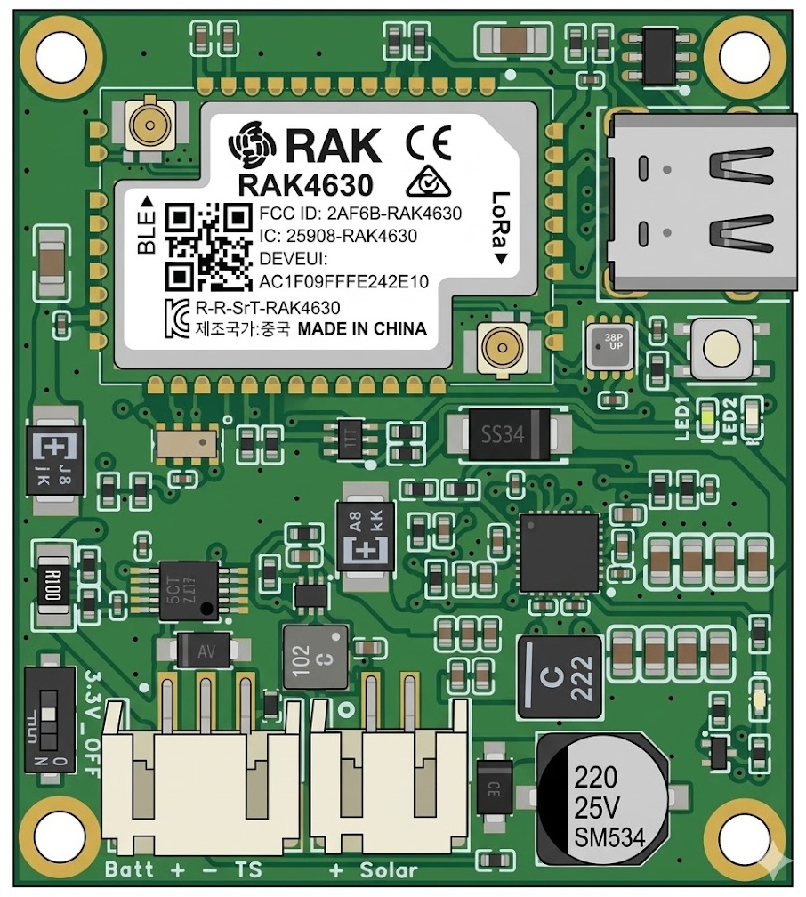
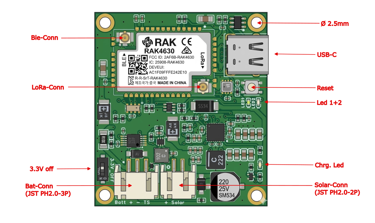
Connectors, Buttons & LEDs – Front Side
| Label (→ image) | Name | Description |
|---|---|---|
| Ble-Conn | U.FL – BLE | Antenna connector for Bluetooth Low Energy (top left on RAK4630) |
| LoRa-Conn | U.FL – LoRa | Antenna connector for LoRa Sub-GHz (left center on RAK4630) |
| USB-C | USB-C Port | USB interface for power supply, charging, firmware flashing and CLI access (top right). CC1/CC2 pulled to GND via 4.7 kΩ (USB sink). VBUS-USB is connected to VBUS-BQ (solar input) via a Schottky diode — USB power feeds the same charger input as the solar panel. |
| Reset | Reset Button | Single click: reset the nRF52840. Double click: enter USB mass storage mode for UF2 firmware updates (right side, below USB-C) |
| Led 1+2 | Status LEDs | LED1 + LED2 = RAK4630 user LEDs (heartbeat / boot indicator, right side, stacked) |
| Chrg. Led | Charge LED | BQ25798 STAT output – indicates charge status (bottom right, next to solar connector) |
| 3.3V off | Power Switch | Slide switch to disconnect the 3.3 V supply (bottom left). ⚠ Caution: Inverted logic! Switch position "ON" = EN pin low = board off. Switch position "OFF" = EN pin high = board on. |
| Bat-Conn (JST PH2.0-3P) | Battery Connector | 3-pin JST PH2.0 connector: Batt+, Batt−, TS (bottom left) |
| Solar-Conn (JST PH2.0-2P) | Solar Connector | 2-pin JST PH2.0 connector: Solar+, Solar− (bottom right) |
| Ø 2.5mm | Mounting Holes | 4× M2.5 mounting holes in the corners |
Key Components – Front Side
| Component | Name | Description |
|---|---|---|
| RAK4630(H) | Core Module | nRF52840 SoC + SX1262 LoRa transceiver, high-band variant (center, shielded) |
| BME280 | Environmental Sensor | Temperature, humidity, pressure |
| BQ25798 | Battery Charger | MPPT, JEITA temperature protection, 15-bit ADC |
| INA228 | Power Monitor | Coulomb counter with ALERT interrupt |
| TPS62840 | Buck Converter | DC/DC, 750 mA, EN switched via 3.3V off switch |
Pinout – Battery Connector (JST PH2.0-3P, left to right)
| Pin | Signal | Description |
|---|---|---|
| 1 | Batt + | Battery positive terminal |
| 2 | Batt − | Battery negative terminal (GND) |
| 3 | TS | Temperature sensor (NTC) for JEITA charge protection. Required type: NCP15XH103F03RC (10 kΩ @ 25 °C, Beta 3380) or compatible |
⚠ WARNING: No reverse polarity protection. Verify correct polarity before connecting.
Pinout – Solar Connector (JST PH2.0-2P, left to right)
| Pin | Signal | Description |
|---|---|---|
| 1 | Solar + | Solar panel positive (3.6 V – 24 V, max. Voc 25 V) |
| 2 | Solar − | Solar panel negative (GND) |
⚠ WARNING: No reverse polarity protection. Verify correct polarity before connecting.
USB Charging Path
USB-C VBUS is connected to the BQ25798 VBUS input (same single input as solar) via a Schottky diode. The BQ25798 has only one VBUS input and does not distinguish between USB and solar. CC1 and CC2 are pulled to GND via 4.7 kΩ resistors, advertising the board as a USB power sink (5 V default). The Schottky diode prevents backflow from the solar panel to the USB bus, but current can flow from USB-VBUS out through the solar connector.
USB Auto-Management
The nRF52840 USB peripheral is automatically managed based on VBUS detection:
- VBUS detected → USB peripheral enabled (Serial available)
- VBUS removed → USB peripheral disabled (saves ~0.8–1.0 mA)
- Boot without USB → USB disabled on first loop iteration
No manual CLI commands are required. USB is always available when a cable is connected. See also FAQ #7 — USB charging.
⚠ Warning: Since VBUS-USB and VBUS-BQ (solar input) are connected via the Schottky diode, a short circuit on the solar connector will also short VBUS-USB. Never short-circuit the solar input while USB is connected.
See also FAQ #16 — 3.3V off switch for practical use cases.
PCB – Back Side
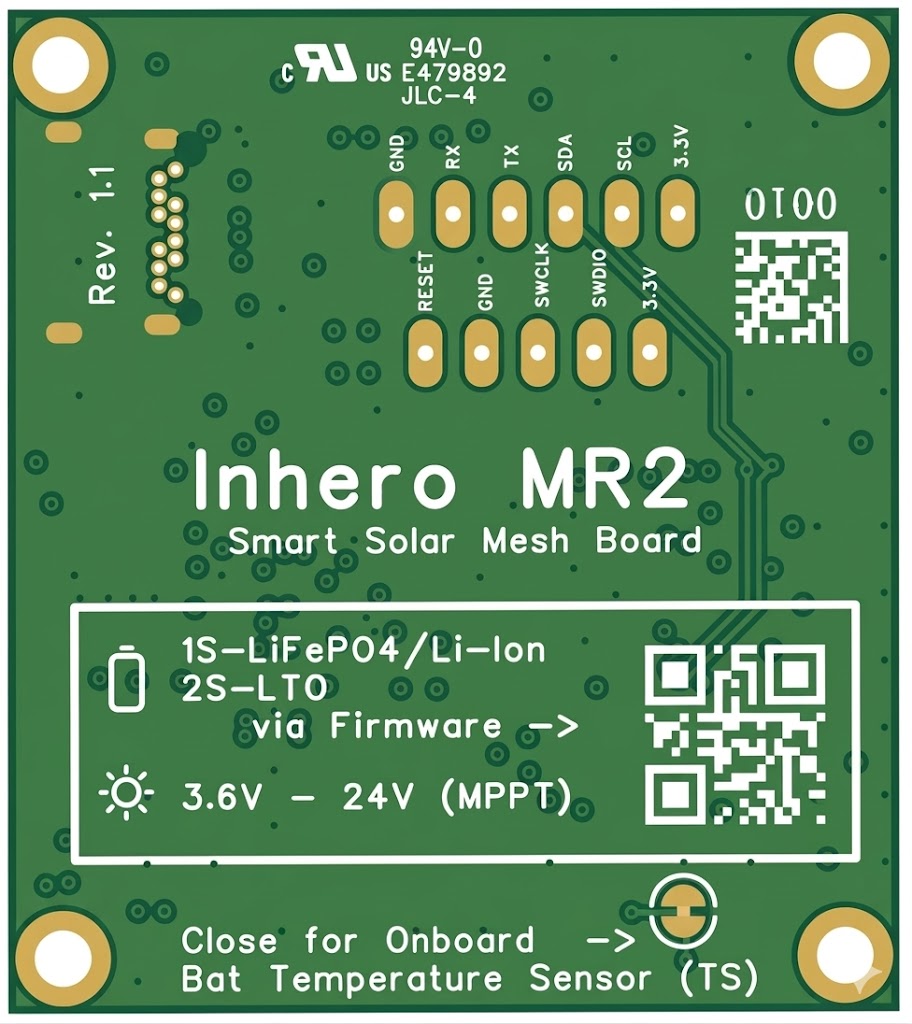
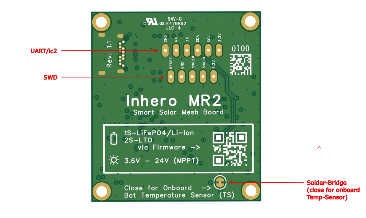
Headers & Pads – Back Side
UART/I2C – Header Row 1 (top row, castellated pads)
| Pin | Signal | Description |
|---|---|---|
| 1 | GND | Ground |
| 2 | RX | UART Receive |
| 3 | TX | UART Transmit |
| 4 | SDA | I2C Data |
| 5 | SCL | I2C Clock |
| 6 | 3.3V | 3.3 V output (max. 500 mA, shared with board consumption) |
SWD – Header Row 2 (bottom row, castellated pads)
| Pin | Signal | Description |
|---|---|---|
| 1 | RESET | nRF52840 Reset |
| 2 | GND | Ground |
| 3 | SWCLK | SWD Clock (debug interface) |
| 4 | SWDIO | SWD Data (debug interface) |
| 5 | 3.3V | 3.3 V output (max. 500 mA, shared with board consumption) |
Solder Bridge – Onboard Temperature Sensor (bottom right)
| Label (→ image) | Description |
|---|---|
| Solder-Bridge (close for onboard Temp-Sensor) | Solder bridge for the onboard NTC temperature sensor (NCP15XH103F03RC, 10 kΩ @ 25 °C, Beta 3380). Closed = onboard NTC active. Open = external NTC of type NCP15XH103F03RC (10 kΩ @ 25 °C, Beta 3380) or compatible required via TS pin on the battery connector. For an installation without an NTC, set board.jeitaignore 1 drops the TS pin from the charge decision, the hot-side suspend included (see the JEITA Override row above). See FAQ #2. |
I2C Bus – Address Map
| Address | Component | Function |
|---|---|---|
| 0x40 | INA228 | Power Monitor / Coulomb Counter |
| 0x52 | RV-3028-C7 | Real-Time Clock (RTC) |
| 0x6B | BQ25798 | Battery Charger (MPPT, JEITA) |
| 0x76 | BME280 | Environmental Sensor (T, H, P) |
Pin Assignment (Key GPIOs)
| nRF52840 Pin | RAK Module Pin | Function |
|---|---|---|
| P0.04 | WB_IO4 | BQ CE pin (via N-FET, inverted) |
| P1.02 | WB_IO2 | INA228 ALERT (low-voltage interrupt) |
| P0.17 | WB_IO1 | RV-3028 RTC interrupt |
| P0.21 | WB_IO3 | BQ25798 INT (unused, polled; pulled up) |
Supported Battery Chemistries
| Type | Nominal Voltage | Charge Voltage | Low-V Sleep | Low-V Wake | Hysteresis |
|---|---|---|---|---|---|
| Li-ion 1S | 3.7 V | 4.1 V | 3100 mV | 3300 mV | 200 mV |
| LiFePO4 1S | 3.2 V | 3.5 V | 2700 mV | 2900 mV | 200 mV |
| LTO 2S | 4.6 V (2× 2.3 V) | 5.4 V | 3900 mV | 4100 mV | 200 mV |
| Na-ion 1S | 3.1 V | 3.9 V | 2500 mV | 2700 mV | 200 mV |
| none | — | — | — | — | — |
Choosing the right chemistry: See BATTERY_GUIDE.md for a detailed comparison of pros, cons, and deployment recommendations. A brief summary is also in FAQ #1.
Firmware Environments
| Build Target | Description |
|---|---|
Inhero_MR2_repeater |
Standard repeater |
Inhero_MR2_repeater_bridge_rs232 |
Repeater with RS232 bridge (Serial2 on P0.19/P0.20) |
Inhero_MR2_sensor |
Sensor firmware |
Absolute Maximum Ratings
| Parameter | Min | Max | Unit |
|---|---|---|---|
| Solar input voltage (Voc) | — | 25 | V |
| Charge current (configurable) | 50 | 1500 | mA |
| Shunt current (INA228, 100 mΩ) | — | 1600 | mA |
| Ambient temperature (operating) | –40 | +85 | °C |
See Also
- README.md – Overview, feature matrix and diagnostics
- TELEMETRY.md — Telemetry channels explained (what the app displays)
- QUICK_START.md – Quick start for commissioning and CLI setup
- BATTERY_GUIDE.md – Battery chemistry comparison and deployment guide
- FAQ.md – Frequently asked questions
- CLI_CHEAT_SHEET.md – All board-specific CLI commands at a glance
- POWER_MANAGEMENT.md – Complete technical documentation